Latent until activated by the correct frequency wavelengh to resonate the cavity.
Viral latency is the ability of a virus to remain dormant within the host cell
A virus receptor can be defined as a host cell surface component recognized by the virus as a gateway to entry into the cell.
Membrane potential is the difference in electric potential between the interior and the exterior of a biological cell.
Cationic liposomes are spherical structures that contain positively charged lipids. Cationic liposomes can vary in size between 40 nm and 500 nm, and they can either have one lipid bilayer (monolamellar) or multiple lipid bilayers (multilamellar).[1] The positive charge of the phospholipids allows cationic liposomes to form complexes with negatively charged nucleic acids (DNA, mRNA, and siRNA) through ionic interactions.
Ionic interactions arise from electrostatic attraction between two groups of opposite charge. ... These interactions do not produce true “bonds,” since there is no sharing of electrons between the groups involved. The groups are pushed together by their “expulsion” from the polar medium.
The dipole consists of two point electric charges of opposite polarity located close together.
An ion-dipole force is an attractive force that results from the electrostatic attraction between an ion and a neutral molecule that has a dipole. Most commonly found in solutions. ... A positive ion (cation) attracts the partially negative end of a neutral polar molecule.
Dipolar or polar molecules are the molecules that posses an electric dipole. The dipoles of some molecules depend on their environment and can change substantially when they are transferred from one medium to another, especially when molecules become ionized in a solvent.
Photoionization is the physical process in which an ion is formed from the interaction of a photon with an atom or molecule.
In some materials, the absorption of a single photon can trigger a chain reaction that produces a large burst of light. The discovery of these photon avalanches in nanostructures opens the way to imaging and sensing applications.
The photon is a type of elementary particle. It is the quantum of the electromagnetic field, including electromagnetic radiation such as light and radio waves and the force carrier for the electromagnetic force. Photons are massless, so they always move at the speed of light in vacuum, 299792458 m/s.
Photon echo is a fundamental tool for the manipulation of electromagnetic fields.
Photon Echo
The signal of the photon echo (PE) is the optical coherent response of a resonant medium (such as a crystal doped with ions) to the effects in certain conditions of two or more laser pulses separated in time.
From: Fundamentals of Femtosecond Optics, 2013
7 Conclusion and Outlook
R-doped crystals fulfill many of the requirements for an efficient QIP system. Protocols exist that take advantage of their specific spectroscopic properties, which can be moreover enhanced and tailored by a number of techniques. In particular, R-doped crystals can provide interfaces between photonic quantum bits, in the optical and microwave ranges, and solid-state qubits. As these qubits can be further processed by optical control, a complete quantum network node could be obtained.
However, a QIP system outperforming a classical system in current information processing tasks is extremely demanding. Still, R-based quantum memories seem much closer to reach the required operating parameters than quantum computers, which are clearly much more complex devices. Strong theoretical and experimental improvements are needed, including development of new materials. Here, bulk single crystals are the preferred choice because of their outstanding spectroscopic properties, although some parameters have still to be improved. Attractive alternatives, like nanostructured materials, may provide additional and important features. In particular, this could allow coupling R ions to other atomic quantum systems, nanoscale quantum mechanical oscillators, or nanocavities.
In such hybrid quantum systems, one could expect to combine efficient processing and storage functionalities, and interface quantum states of different physical nature. This approach may not only benefit QIP but also open the way to fundamental studies in quantum physics.
5.2.2 Crystals
The only Tm3 +-doped crystal system studied so far has been BaY2F8:Tm3 +. In 2004, Patterson et al. reported laser cooling of a Tm3 +-doped crystal for the first time (Patterson et al., 2004). They used a BaY2F8:Tm3 + crystal grown by the Czochralski method and pumped it in single-pass geometry using a high-power OPO with 4–6 W output power in the 1700–2100 nm tuning range to achieve cooling by ~ 1.5 K when pumping at 1902 nm. A second study by Patterson et al. used a high-purity BaY2F8 crystal doped with 1.2% Tm3 + pumped in single-pass geometry (Patterson et al., 2008).
They measured a mean fluorescence wavelength of 1793 nm at room temperature and pointed out the advantageous higher peak absorption cross sections afforded by the crystalline host compared to the amorphous ZBLAN samples studied earlier. The measurement of normalized temperature drop for different pump wavelengths is shown in Fig. 25 and indicates maximum cooling at 1855 nm, where a net temperature drop of 3.2 K was obtained with 4.4 W of pump power. The solid curve shown in Fig. 25 is a fit to the experimental data and yielded a quantum efficiency of η = 0.98 and a background absorption coefficient of 2 × 10− 4 cm− 1. The cooling efficiency was highest with 3.4% at a pump wavelength of 1934 nm.
Ultrafast spin dynamics in the ground state of a rare‐earth‐ion doped crystal are studied by the polarization spectroscopy with the optical pump‐probe technique. Quantum‐ beat FID signals in the subnanosecond region were observed. Their Fourier transform gives the ESR spectra. The spin‐lattice relaxation time T1 is obtained from the decay curve of the optically‐induced magnetization up to the room temperature, where the relaxation time is of the order of picoseconds. The observed temperature dependence of the rate 1/T1 near room temperature deviates from the well‐known T9 dependence. Considering the effect of the Debye temperature of the host crystal on the Raman process, the observed temperature dependence of 1/T1 can be explained well. Ultrafast spin dynamics such as observed in the present work cannot be observed by the conventional ESR, whose time resolution is nanoseconds at best.
Optical Nuclear Polarization
In 1967, Maier and Wolf observed nuclear hyperpolarization in pure anthracene single crystals upon illumination with unpolarized white light. Later the effect was also found in doped crystals of other condensed aromatic compounds. The effect has a maximum at rather low fields (around 0.01 T), although it often remains observable at higher fields. Mostly samples are polarized outside the magnet and, due to long T1, transferred conveniently into the magnet for the NMR measurement.
It has been shown that the origin of the optical nuclear polarization (ONP) is electron hyperpolarization, called optical electron polarization (OEP), occurring in the triplet state.
Upon light excitation, excited electronic singlet states are populated (Scheme 4). Intersystem crossing (ISC) allows for population of electronic triplet states. Owing to zero field splitting (ZFS), in molecules the three triplet electron states are not degenerate.
As pointed out by Wolf and van der Waals in the late 1960s, spin-orbit coupling pathways allowing for ISC are highly spin selective. Therefore, often only one of these three electronic triplet states is populated – the one that has the symmetry matching the preceding excited singlet state. Similarly, the decay to the ground state S0 is controlled by spin-selective ISC. Hence, non-Boltzmann electron population and therefore electron hyperpolarization is created.
This electron hyperpolarization can be transferred to nuclear hyperpolarization by static hyperfine coupling during the lifetime of the triplet state. As shown by both Veeman and Stehlik, the optimum polarization transfer to nuclei can be reached if a selective mixing of the electronic triplet states by a hyperfine interaction occurs, which leads to level anticrossing (LAC) by conserving the total magnetic quantum number. In molecular crystals, migration of triplet excitations and their trapping may control the kinetics and site of the occurrence of ONP.
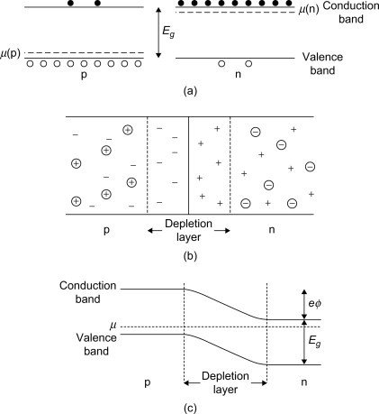
A simple p-n junction is fabricated by taking a single intrinsic semiconductor such as Si in which donor impurities are introduced in one region and acceptor impurities are introduced into another.
It is easier to visualize the p-n junction as equivalent to two Si crystals doped with donor (n-type) and acceptor (p-type) impurities joined together with polished surfaces. In practice, this is not a good idea because the surface effects would interfere with the properties of the semiconductor. These semiconductors have different chemical potentials, respectively. Initially, most of the conduction electrons are at the n-type, and the holes are at the p-type semiconductor.
This scenario is shown in Figure 10.3a. However, when the two materials are joined together, some of the conduction electrons will diffuse to the p-type material while some of the holes will diffuse to the n-type material. When an electron diffuses to the p-type layer, it will recombine with a hole due to the large concentration of holes in that layer. A similar situation will arise when a hole diffuses to the n-type layer. As more and more electrons and holes diffuse to the p- and n-type layers, the number of carriers in the junction will be greatly reduced. Thus, the layer on either side of the junction has much lower concentration of carriers than the rest of the semiconductor. This is known as the depletion layer, which is shown in Figure 10.3b and usually has an approximate length of
Å
We note that the donor and acceptor ions are much too heavy to diffuse like the electrons and holes. Thus, the p-n junction is formed in the semiconductor with a common chemical potential
This is shown in Figure 10.3c.
Figure 10.3. (a) The electrons (solids) and holes (open circles) in p- and n-type semiconductors. (b) When the p- and n-type regions are in contact, there are practically no carriers in the depletion region. The acceptor and donor ions are represented by circles with signs. (c) The distribution of charge at a p-n junction produces a contact potential across the junction.
4 Electrical characterization
Resistivity, magnetoresisitance and Hall effect were measured on β-FeSi2 crystals from room temperature (RT) down to below 20 K. The magnetic field strength was in the range 0.1 to 0.8 T, a standard value was 0.495 T. Ohmic contacts were made by a Pt adhesive. Bridge and van der Pauw configurations were used. Fig. 2 shows the dependence of the resistivity ρ on temperature for undoped crystals and for crystals doped with Cr, Mn, Co and Ni. All the samples revealed semiconducting behaviour. Values of ρ were in the range between 0.2 and nearly 100 Ωcm at RT, and between nearly 100 and 1000 Ωcm at 11 K. We found p-type behaviour in all samples from the sign of the Hall-coefficient.
The expected n-type conductivity caused by Co or Ni doping was not observed. This is not surprising considering that Cr and Mn were main impurities in the starting powder and that only about 0.1 at.% of the dopants added were built in. For Cr-doped samples there is a shoulder in ρ at about 70–100 K. From RT to the shoulder there is a steep increase of ρ. At lower temperatures the ρ(T) curve is similar to those for the other samples. The magnetoresistance ΔρMF was measurable at low temperatures only. It exhibited negative sign.
In a Ni-doped sample we found ΔρMF = −0.1% (B = 0.2 T) and ΔρMF= −0.16% (B = 0.6 T). The negative magnetoresistance is related to variable-range hopping [6] or to a magnetic order effect [7]. At RT the determination of the Hall coefficient RH for most samples was difficult because of the low mobility observed. For Cr-doped samples RH values > 1 cm3 per As led to free carrier concentrations of some 1018 cm−3 and typical mobilities of 10 cm2 per Vs. Fig. 3 shows the temperature dependence of hole concentration of several crystals doped with Cr. Below RT there is a strong freeze out of free carriers which can be described well within the frame of Fermi statistics. An activation energy of the Cr acceptor of 75 ± 10 meV was determined as an average of four values. Between 75 and 100 K the free carrier concentration exhibits a much slower decrease with temperature which cannot be explained by a simple one-band-one-acceptor model. For a more detailed discussion of this problem see Ref. [8].
🤦🏼♂️👉🏻❤️
Semiconductor quantum dots (QDs) has attracted considerable interest since a few years. To be part of photonic structures QDs are generally embedded in thin films. After briefly reviewing the field of nanophotonics, modeling of the electronic properties of QDs based on the effective mass approximation is presented. Examples of results concerning optical properties of PMMA thin films containing CdSe/ZnS and TiO2 QDs are given describing their reflection, transmission, absorption, and photoluminescence. The problem of the refractive index of thin films containing QDs and of QDs alone is also addressed. Finally, we discuss application of QDs layers for solar cells, lighting and displays, and in optical interference coatings for extra high reflection and transmission coefficients.
12.1 Introduction
Semiconductor quantum dots (QDs) are nanoscale material clusters composed of 102–105 atoms. The size of the QDs is orders of magnitude larger than a typical atomic radius, yet small enough to provide quantum confinement of electrons and holes in all three spatial dimensions. Consequently, they are also referred to as artificial atoms. A unique property of the semiconductor QDs is that the energies and wave functions of the quantum confined states can be tailored by controlling their size, shape, and composition.
The semiconductor QDs are typically fabricated either by chemical synthesis or epitaxial growth. The chemical fabrication methods have the advantage of being inexpensive, but the epitaxial QDs have several important benefits, including the possibility of direct integration in a high quality crystalline matrix, which provides high optical quality and enables fabrication of optical and electrical devices exploiting epitaxial heterostructure technology.
The most widely explored type of epitaxial semiconductor QDs are the coherently strained epitaxial InAs QDs obtained by Stranski-Krastanov growth on GaAs surfaces (Moison et al., 1994;, Madhukar et al., 1994; Leonard et al., 1994). A single InAs/GaAs QD has proven to be a beneficial model system for a broad field of experimental quantum mechanics, including the studies of light-matter interaction and cavity quantum electrodynamics (Yoshie et al., 2004) as well as coherent control experiments (Dory et al., 2016).
From application point of view, significant effort has been dedicated to the development of efficient single-QD-based sources of nonclassical light for producing single, entangled (Chen et al., 2016) or indistinguishable (Santori et al., 2002) photons on demand for application in quantum communication and cryptography. Such applications usually require integration of QDs in optical microcavities or other small-scale photonic structures in order to obtain high brightness and efficient photon extraction. In turn, this requires precise positioning of the QD with respect to the photonic structures in order to enable interaction with the strongly localized fields of the microcavity modes. To this end, site-controlled epitaxy has emerged as a favorable fabrication approach enabling deterministic control of the QD nucleation sites and providing additional possibilities for tuning the QD properties.
7 Inorganic Optical Core Coated With a Silica Shell
Semiconductor quantum dots (QDs) have a broad absorption band and a narrow tunable emission band, depending on their sizes. As was shown earlier, semiconductor QDs have a great potential for live cell visualization and early cancer detection [54,55]. On the other hand, semiconductor QDs are considered to be toxic, mainly due to the atoms of heavy elements in their composition [56]. Therefore, a similar core-shell coating strategy can be adopted to reduce the QD toxicity. In particular, the toxicity of CdSe/CdS/ZnS QDs was significantly reduced after a silica coating [57]. Furthermore, the resultant silica-coated QDs showed excellent long-term photo and colloidal stability, even in some harsh environments. Nearly similar results were also reported by another research group [58].
According to their results, the silica-coated CdSe QDs were nontoxic even at relatively high loadings (up to 1000 nM). At the same time, silica coating can be used to enhance the optical properties of some optical materials. For example, Zhang and coworkers showed that the quantum yield of some QDs with appropriate structure and composition could be enhanced after a silica coating [58]. Therefore, silica coating can highly reduce the QD toxicity and enhance their fluorescent properties. The luminescence enhancement can also be observed in the case of phosphor materials.
In this case, the inert and optically transparent silica coating can protect the phosphors from luminescence killers such as water and air. For instance, Gd2O3-based phosphors used for biomedical applications should always be coated with silica, for two reasons. First, leaching of free Gd3 + ions is quite dangerous for living cells [59]. Second, the luminescent signal of Gd2O3-based phosphors can be reduced in the presence of water molecules [60].
Lü and coworkers showed that the two-photon upconversion emission spectra of Y2O3:Eu3 + can be improved after a silica coating [61]. Atabaev and coworkers also observed the luminescence enhancement of Y2O3:Eu3 +, Co2 + NPs after a silica coating process [62]. Thus, the phosphors with improved luminescent properties can be used for optical devices and biotechnology. In some cases, researchers combined both magnetic and optical NPs in one silica nanoparticle [63]. The fluorescent silica shell layer on the surface of other optical materials can be used in sensing applications. For example, the FITC-doped silica shell was coated on the surface of Y2O3:Eu3 + [42] and rhodamine B dye-doped Fe3O4@SiO2 [64] nanostructures.
These nanostructures can be used for ratiometric pH detection, where the inner optical core serves as a reference and the outer shell layer serves as a pH indicator. Thus, thanks to the simple silica coating design, it has become possible to obtain biocompatible NPs with a large range of functionalities.
5.2.2.2 Semiconductor Quantum Dot Inks
Semiconductor QDs have recently received great attention because of their high photochemical stability and size-dependent optical properties, which result from the quantum-confinement effect (Elliott et al., 2013; Haverinen, Myllyla, & Jabbour, 2009, 2010; Kim et al., 2009; Tekin et al., 2007; Wood et al., 2009). More importantly, the color of the photoluminescence of the QDs can be tuned easily by varying their sizes. Due to these unique properties, the QDs are widely used in optoelectronic devices such as high-efficiency luminescent devices, light-emitting devices, and photovoltaic cells.
To integrate the QDs with these solid-state devices, they must be precisely patterned in predetermined locations on substrates. Presently, there have been various methods to pattern the QD nano-inks. Among these methods, inkjet-printing is particularly attractive because of its additive approach, which allows significant cost savings, increased choice of substrates, and the ability of multiple depositions on one substrate. Figure 5.7 lists several examples of the inkjet-printing of semiconductor QD nano-inks for the purpose of fabricating luminescent patterns.
Figure 5.7(a) demonstrates that luminescent nanocrystal–polymer nanocomposites are printed to produce well-defined dot arrays (Tekin et al., 2007). By using the single-nozzle system and the multi-nozzle system, single-color array and multicolor pixel patterns are printed, respectively. Green, orange, and red emissions of the patterns are realized by adding differently sized CdSe@ZnS QDs into the printing inks. In this work, the color of each printed pixel is fixed. To realize more abundant color displaying, combinatorial libraries of nanocrystals with different sizes are used as printing inks.
The photograph of an inkjet-printed combinatorial library of different size CdTe nanocrystals emitting at different wavelengths and their photoluminescence spectra are shown in Figure 5.7(b). By adjusting the ratio of the differently sized nanocrystals in the inks, more complicated colors will be displayed (Kim et al., 2009). As shown in Figure 5.7(c), full-color displays can be fabricated by printing the red, green, and blue light-emitting QD nanocomposite inks. The efficient and stable QD phosphor inks result in robust, bright, and highly reliable displays. Moreover, the inkjet-printed QD patterns are well suited for integration with the underlying metal oxide dielectric substrates that can further improve the optical and electrical performance of the devices (Wood et al., 2009).
15.3.1 Dielectric microresonators with colloidal quantum dots
Semiconductor quantum dots typically have diameters of a few nanometers, which are two orders of magnitude smaller than the wavelength of visible light. One way to increase the interaction of a quantum dot with the light field is using a microcavity. Fabrication of pillar microcavities made of semiconductor material and containing self-assembled quantum dots is well established.20 In contrast, technologies for the implementation of colloidal semiconductor quantum dots into dielectric microcavities had yet to be developed.
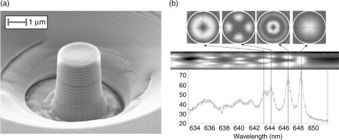
We have manufactured high-quality pillar resonators with embedded colloidal CdSe/ZnS quantum dots as light emitters by focused ion beam (FIB) milling (Fig. 15.6a).23 First, a planar dielectric cavity is formed by two Bragg mirrors, each consisting of sputtered pairs of alternating TiO2 and SiO2 λ/4 layers. The centre of the cavity hosts colloidal CdSe/ZnS quantum dots that are mixed into liquid polysilazane. After solidification of this layer the dots are embedded in a robust SiO2 layer of λ/2 thickness.
Subsequently, micropillars with diameters in the range of 2.4 μm down to 600 nm are milled out of the planar cavity via FIB. A broadband light transmission measurement through a single micropost resonator showed the lowest cavity mode blue-shifting with decreasing pillar diameters. This effect nicely demonstrates three-dimensional light confinement.
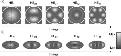
Higher cavity modes are clearly visible in the PL emission from the quantum dot ensemble (Fig. 15.6b). The spectral positions of these resonances are calculated by modeling the pillar cavity as a waveguide with an effective refractive index. First, the electric field amplitude in the direction perpendicular to the layers is computed. We use the transfer-matrix method to determine the longitudinal modes in a planar cavity with the identical sequence of the layers as for the pillar resonator.
Second, the entire pillar cavity is characterized by an effective refractive index neff. We average over the entire pillar cavity by weighting the refractive index at each point in space with the longitudinal electric field amplitude: neff = ∫ n(z). |E(z)2|/max |E(z)|2. Third, the electromagnetic field in the lateral direction is calculated by modeling the pillar microcavity as a homogenous dielectric waveguide. It has a cylindrical shape with index of refraction neff. The cavity modes of the pillar are now easily retrieved by solving the transverse wave equation.24 As seen in Fig. 15.6b, the theoretical results are in excellent agreement with the pillar mode positions observed in the experiments.
Nothing to see here...


