What good is a mask unless it is a photomask?
...as the vaccine is activated through the eyes?
Bastards.
Blunt to the point of abrasive..I shoot from the hip.. AM directed by the heart .. tempered by the 🧠
woukd ray bans help??
New @percatateya at X - Phd Social & Labour Psychology ER Responder - This is about the World. Avatar Master, Uruguay, South America.
Blackbody radiation refers to the spectrum of light emitted by any heated object; common examples include the heating element of a toaster and the filament of a light bulb.
A black body or blackbody is an idealized physical body that absorbs all incident electromagnetic radiation, regardless of frequency or angle of incidence. The name "black body" is given because it absorbs all colors of light. A black body also emits black-body radiation.
Lattice gauge theory is an essential tool for strongly interacting non-Abelian fields, such as those in quantum chromodynamics where lattice results have been of central importance for several decades. Recent studies suggest that quantum computers could extend the reach of lattice gauge theory in dramatic ways, but the usefulness of quantum annealing hardware for lattice gauge theory has not yet been explored. In this work, we implement SU(2) pure gauge theory on a quantum annealer for lattices comprising a few plaquettes in a row with a periodic boundary condition. These plaquettes are in two spatial dimensions and calculations use the Hamiltonian formulation where time is not discretized. Numerical results are obtained from calculations on D-Wave Advantage hardware for eigenvalues, eigenvectors, vacuum expectation values, and time evolution.
The success of this initial exploration indicates that the quantum annealer might become a useful hardware platform for some aspects of lattice gauge theories.
Quantum annealing starts from a quantum-mechanical superposition of all possible states (candidate states) with equal weights. Then the system evolves following the time-dependent Schrödinger equation, a natural quantum-mechanical evolution of physical systems. The amplitudes of all candidate states keep changing, realizing a quantum parallelism, according to the time-dependent strength of the transverse field, which causes quantum tunneling between states. If the rate of change of the transverse field is slow enough, the system stays close to the ground state of the instantaneous Hamiltonian (also see adiabatic quantum computation).[6]
If the rate of change of the transverse field is accelerated, the system may leave the ground state temporarily but produce a higher likelihood of concluding in the ground state of the final problem Hamiltonian, i.e., diabatic quantum computation.[7][8] The transverse field is finally switched off, and the system is expected to have reached the ground state of the classical Ising model that corresponds to the solution to the original optimization problem. An experimental demonstration of the success of quantum annealing for random magnets was reported immediately after the initial theoretical proposal.[9]
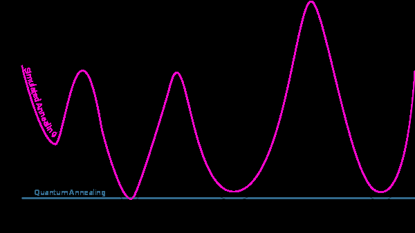
Quantum Annealing (blue line) efficiently traverses energy landscapes by leveraging quantum tunneling to find the global minimum. Quantum annealing offers a significant performance advantage over Simulated Annealing (magenta line), unlocking the potential to solve massive optimization problems previously thought to be impossible.
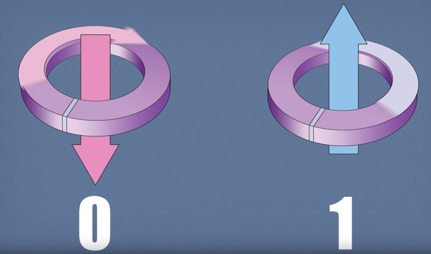
One of the main differences between classical computers and quantum computers is the use of the qubit. The computers we are accustomed to use bits, which is a binary digit that can either have a value of 0 or 1. A qubit can be any two level quantum system, such as a spin in a magnetic field or a single photon. Similar to a bit, a qubit has a possible value of 0 or 1. However, in the quantum world a qubit can be in both states at once (superposition).
The wikipedia definition of quantum superposition states, “any two (or more) quantum states can be added together (“superposed”) and the result will be another valid quantum state; and conversely, that every quantum state can be represented as a sum of two or more other distinct states”. The two states in this definition for the qubit are the 0 or 1 values a normal bit can also have. Basically, before a qubit is observed it is in a superposition of probabilities for 0 and 1. A great example to help explain this is to picture a coin being flipped vs a coin being spun. If you flip a coin it will land on either heads or tails (bit). However, while a coin is spinning you can say the coin’s state is both heads and tails at the same time (qubit). The catch is that once a qubit is observed it will take of the state of either 1 or 0. The video below does a much better job explaining how a qubit works and helps explain superposition.
The thermal radiation of small conducting particles was investigated in the region where the Stephan-Boltzmann law is not valid and strongly overestimates radiation losses. The new criterion for the particle size, at which black body radiation law fails, was formulated. The critical radius rc is expressed through a combination of temperature T and particle conductivity σ: thus rc = c(ћ/2πσkT)1/2. The approach is based on the magnetic particle polarization, which is valid until very small sizes (cluster size) where due to drop of particle conductivity the electric polarization prevails over the magnetic one. It was also shown that the radiation power of clusters, estimated on the basis of the experimental data, is lower than that given by the Stephan-Boltzmann law.
In the last years the amount of research in the field of nanotechnology, nanomaterials and nanosystems tremendously increased [1]. One of the most important trends in the nanotechnology is obtaining and using of nanopowders, which can be used in metallurgy, microelectronics, and medicine and food industry. Production and processing of nanopowders are frequently dealt with heating of nanoparticles to high temperatures when intensive thermal radiation can be expected.
The problem is close related to dust plasma [2], and to the role of dust in fusion devices [3], where micro- and nano- particles are heated to high temperatures and radiation energy losses can play decisive role in the energy balance of the particles. The effect of metal clusters on emission spectra was discussed in [4].
1
The black body radiation cannot be used for the calculation of nanoparticle energy balance, because for the particles smaller than radiation wavelength the Stephan-Boltzmann formula gives far overestimated results.
Thermal radiation of conducting nanoparticles
Yu.V.Martynenko, L.I.Ognev
Nuclear Fusion Institute, Russian Research Center “Kurchatov Insitute”, 123182, Moscow, Kurchatov sq., 1
Thermal radiation is electromagnetic radiation generated by the thermal motion of particles in matter. Thermal radiation is generated when heat from the movement of charges in the material is converted to electromagnetic radiation. All matter with a temperature greater than absolute zero emits thermal radiation
"Thermal radiation is generated
when heat from the movement of charges
in the material
is converted
to electromagnetic radiation"
Moving charges are in fact the source of magnetic fields, whether charges moving deep inside a bar magnet or the magnetic field created by a current-carrying wire. But moving charges are also affected by external magnetic fields. When you send a charge through a field created by something else, it will feel a force.
A metamaterial (from the Greek word μετά meta, meaning "beyond" or "after", and the Latin word materia, meaning "matter" or "material") is any material engineered to have a property that is not found in naturally occurring materials.[3] They are made from assemblies of multiple elements fashioned from composite materials such as metals and plastics. The materials are usually arranged in repeating patterns, at scales that are smaller than the wavelengths of the phenomena they influence. Metamaterials derive their properties not from the properties of the base materials, but from their newly designed structures. Their precise shape, geometry, size, orientation and arrangement gives them their smart properties capable of manipulating electromagnetic waves: by blocking, absorbing, enhancing, or bending waves, to achieve benefits that go beyond what is possible with conventional materials.
A superlens, or super lens, is a lens which uses metamaterials to go beyond the diffraction limit. For example, in 1995, Guerra[1] combined a transparent grating having 50nm lines and spaces (the "metamaterial") with a conventional microscope immersion objective. The resulting "superlens" resolved a silicon sample also having 50nm lines and spaces, far beyond the classical diffraction limit imposed by the illumination having 650nm wavelength in air. The diffraction limit is a feature of conventional lenses and microscopes that limits the fineness of their resolution depending on the illumination wavelength and the numerical aperture NA of the objective lens. Many lens designs have been proposed that go beyond the diffraction limit in some way, but constraints and obstacles face each of them.[2]
In 1873 Ernst Abbe reported that conventional lenses are incapable of capturing some fine details of any given image. The super lens is intended to capture such details. The limitation of conventional lenses has inhibited progress in the biological sciences. This is because a virus or DNA molecule cannot be resolved with the highest powered conventional microscopes. This limitation extends to the minute processes of cellular proteins moving alongside microtubules of a living cell in their natural environments. Additionally, computer chips and the interrelated microelectronics continue to be manufactured to smaller and smaller scales. This requires specialized optical equipment, which is also limited because these use conventional lenses. Hence, the principles governing a super lens show that it has potential for imaging DNA molecules, cellular protein processes, and aiding in the manufacture of even smaller computer chips and microelectronics.[3][4][5][6]
Furthermore, conventional lenses capture only the propagating light waves. These are waves that travel from a light source or an object to a lens, or the human eye. This can alternatively be studied as the far field. In contrast, a superlens captures propagating light waves and waves that stay on top of the surface of an object, which, alternatively, can be studied as both the far field and the near field.[7][8]
In the early 20th century the term "superlens" was used by Dennis Gabor to describe something quite different: a compound lenslet array system.[9]
Photosensitive epilepsy is when seizures are triggered by flashing lights or contrasting light and dark patterns.
The word seizure is derived from the Greek meaning “to take hold.”
ray
/reɪ/
MUSIC
noun: re
(in tonic sol-fa) the second note of a major scale.
the note D in the fixed-doh system.
Origin
Middle English re, representing (as an arbitrary name for the note) the first syllable of resonare, taken from a Latin hymn (see solmization).
The god who personified the sun was one of the most important and widely-venerated of Egypt's deities. Re was considered a demiurge, or creator god, who brought himself and the rest of the pantheon into being at the beginning of time. He was also central to the ideology of kingship.
By definition, “to seize the moment” is to take full advantage of life's opportunities whenever and wherever they present themselves; to live life to one's full potential but in retrospect I feel it is more-so a philosophy which you could take as being the opposite of letting opportunities pass you by or of hesitating ...
Electric Potential of a Dipole
Electric dipole moment is represented by a vector p of magnitude 2qa and this vector points in direction from -q to +q. To find electric potential due to a dipole consider charge -q is placed at point P and charge +q is placed at point Q as shown below in the figure.
The prototype, created in 1936 and known as "Anti-Glare", had plastic frames and green lenses that could cut out the glare without obscuring vision. The name "Ray-Ban" was hence derived from the ability of these glasses to limit the ingress of either ultra-violet or infra-red rays of light.
Group III-nitride semiconductor-based ultraviolet (UV) light emitting diodes have been suggested as a substitute for conventional arc-lamps such as mercury, xenon and deuterium arc-lamps, since they are compact, efficient and have a long lifetime. However, in previously reported studies, group III-nitride UV light emitting diodes did not show a broad UV spectrum range as conventional arc-lamps, which restricts their application in fields such as medical therapy and UV spectrophotometry. Here, we propose GaN quantum dots (QDs) grown on different facets of hexagonal truncated pyramid structures formed on a conventional (0001) sapphire substrate.
A hexagonal truncated GaN pyramid structure includes {10[1 with combining macron]1} semipolar facets as well as a (0001) polar facet, which have intrinsically different piezoelectric fields and growth rates of GaN QDs. Consequently, we successfully demonstrated a plateau-like broadband UV spectrum ranging from ∼400 nm (UV-A) to ∼270 nm (UV-C) from the GaN QDs. In addition, at the top-edge of the truncated pyramid structure, a strain was locally suppressed compared to the center of the truncated pyramid structure. As a result, various emission wavelengths in the UV range were achieved from the GaN QDs grown on the sidewall, top-edge and top-center of hexagonal truncated pyramid structures, which ultimately provide a broadband UV spectrum with high efficiency.
Autism spectrum disorder (ASD) is a developmental disability caused by differences in the brain. People with ASD often have problems with social communication and interaction, and restricted or repetitive behaviors or interests. People with ASD may also have different ways of learning, moving, or paying attention.
This is f breaking my heart.
The varied applications of nanotechnology have paved way for several breakthroughs in the realm of biomedical technology. In this challenging era when illness multiplies, timely and accurate disease diagnosis is very important. Thus, well founded novel approaches matter very much in areas like disease diagnosis and monitoring. Nanomedicine has tremendous implications in the given context. An elevated cholesterol concentration in blood is risky and is associated with cardiovascular diseases (CVD). CVD remains the No. 1 global cause of death and hence there is an urge to understand cholesterol level and take preventive measures.
Highly fluorescent graphene quantum dots (GQs) are well known for their biocompatibility, non toxicity and aqueous solubility. Here in we report an easy and sensitive non enzymatic based cholesterol detection using digitonin conjugated graphene quantum dots (GDG). Selectivity studies and the cholesterol detection in human blood serum suggests the probe to be reliable and selective for blood cholesterol monitoring. Digitonin conjugated fluorescent graphene quantumdots, an efficient probe for cholesterol sensing
A C HOLE STER OL S IN S IN G
Tunable-focus liquid crystal (LC) microlens array has become an essential optical component for image processing [1–12], beam steering [13–15], wavefront correction [16] and switchable 2D/3D displays [17–19]. A key to tune the focal length is to create parabolic phase profile by spatially controlling the LC director reorientations, such as introducing inhomogeneous electric field distribution or creating gradient pretilt angle alignment [20,21]. To do so, several approaches have been developed, including curved electrodes [22], patterned electrodes [23], polymer-stabilization [24], composite alignment [25], and composite lenses [26], just to name a few. As for the composite lenses, a reliable way of generating LC alignment on the polymer microlens array is crucial. Other than the traditional rubbing [26] and photoalignment methods [27], here we propose a new fabrication method to fulfil this goal with recently developed two-photon polymerization based direct-laser writing.
They wanted revenge, to right the wrong that had been done to them.
In this paper, we apply direct-laser writing technique to polymerize a parabolic-shape microlens array on an indium tin oxide (ITO)-coated planar substrate. Such a parabolic-shape polymer surface not only generates the desired inhomogeneous electric field for a lens but also serves as LC alignment layer. By filling a LC mixture into the homogeneous alignment-like cell, the focal length of the microlens array is tunable by the applied voltage. In experiment, a 16 ×
16 microlens array with individual microlens size of 120 ×
120 µm2 is fabricated.
The voltage dependent focal length at different wavelengths is measured. The fabricated sample exhibits a conformal pretilt-angle, as evidenced by characterizing the phase profiles under different voltages. The focusing property at different wavelengths and the white-light imaging capability of the microlens array are also investigated. Through this work, it is evident that the direct-laser writing is a viable approach for simultaneously forming curvilinear-surface structure and patterning LC alignment on such a surface. It offers a new option for making other tunable LC photonic devices.
Photonic devices are components for creating, manipulating or detecting light. This can include laser diodes, light-emitting diodes, solar and photovoltaic cells, displays and optical amplifiers.
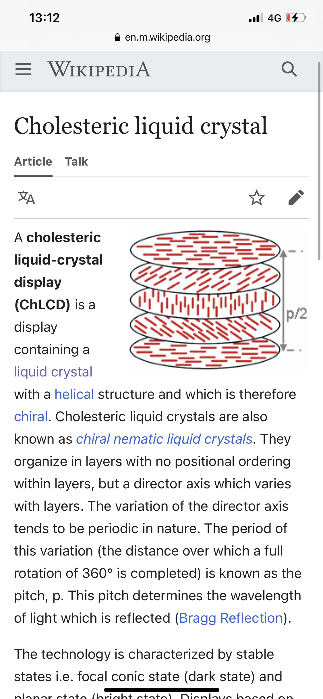
Liquid crystals are complex fluids that allow exquisite control of light propagation thanks to their orientational order and optical anisotropy. Inspired by recent advances in liquid-crystal photo-patterning technology, we propose a soft-matter platform for assembling topological photonic materials that holds promise for protected unidirectional waveguides, sensors, and lasers. Crucial to our approach is to use spatial variations in the orientation of the nematic liquid-crystal molecules to emulate the time modulations needed in a so-called Floquet topological insulator.
The varying orientation of the nematic director introduces a geometric phase that rotates the local optical axes. In conjunction with suitably designed structural properties, this geometric phase leads to the creation of topologically protected states of light. We propose and analyze in detail soft photonic realizations of two iconic topological systems: a Su–Schrieffer–Heeger chain and a Chern insulator. The use of soft building blocks potentially allows for reconfigurable systems that exploit the interplay between topological states of light and the underlying responsive medium.
It is not expedient for me doubtless to glory. I will come to visions and revelations of the Lord.
RE V EL AT IONS

