
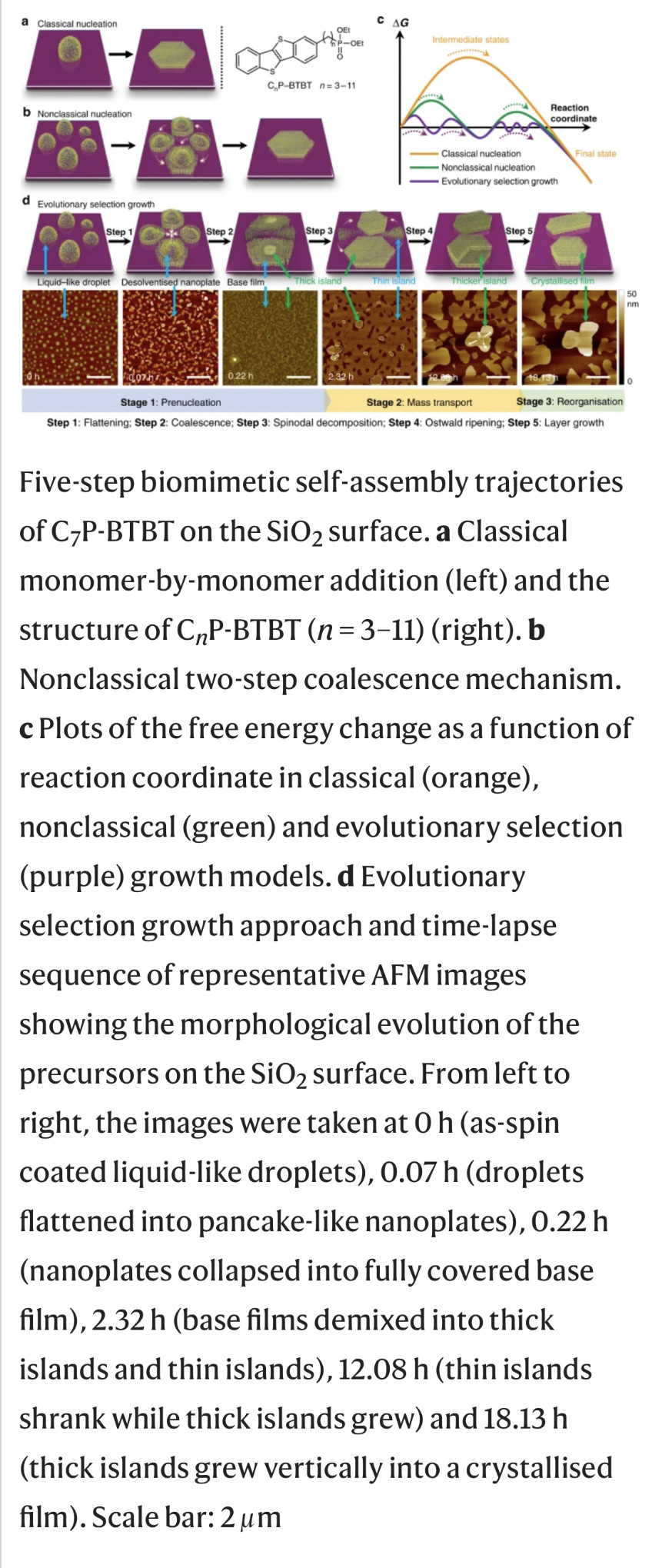
Epitaxy refers to a type of crystal growth or material deposition in which new crystalline layers are formed with one or more well-defined orientations with respect to the crystalline seed layer. The deposited crystalline film is called an epitaxial film or epitaxial layer. The relative orientation(s) of the epitaxial layer to the seed layer is defined in terms of the orientation of the crystal lattice of each material. For most epitaxial growths, the new layer is usually crystalline and each crystallographic domain of the overlayer must have a well-defined orientation relative to the substrate crystal structure. Epitaxy can involve single-crystal structures, although grain-to-grain epitaxy has been observed in granular films.
For most technological applications, single domain epitaxy, which is the growth of an overlayer crystal with one well-defined orientation with respect to the substrate crystal, is preferred. Epitaxy can also play an important role while growing superlattice structures.
A superlattice is a periodic structure of layers of two (or more) materials. Typically, the thickness of one layer is several nanometers. It can also refer to a lower-dimensional structure such as an array of quantum dots or quantum wires.
If the superlattice is made of two semiconductor materials with different band gaps, each quantum well sets up new selection rules that affect the conditions for charges to flow through the structure. The two different semiconductor materials are deposited alternately on each other to form a periodic structure in the growth direction. Since the 1970 proposal of synthetic superlattices by Esaki and Tsu,[11] advances in the physics of such ultra-fine semiconductors, presently called quantum structures, have been made. The concept of quantum confinement has led to the observation of quantum size effects in isolated quantum well heterostructures and is closely related to superlattices through the tunneling phenomena. Therefore, these two ideas are often discussed on the same physical basis, but each has different physics useful for applications in electric and optical devices.